Imprint Lithography
Imprint Lithography Key FeaturesThree Different Imprint Technologies: SCIL, SMILE and UV-NILExtensive Imprint Expertise & Centre of ExcellenceImprint Solutions for R&D to ProductionSmall through Full Area Imprint Solutions
SUSS MicroTec offers various approaches to the imprint technology, tailored to the specific process requirements of different applications.
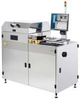
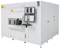
All imprint solutions are based on SUSS Microtec's proven, industry standard semi-automated mask aligner suite and support multiple substrate materials and sizes from small pieces up to 200mm wafers.
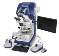
Using the high precision capabilities of SUSS Microtec's mask aligners provides several advantages to the imprint process; accurate stamp to substrate alignment, precise stamp to substrate levelling (via WEC); contact pressure control; convenient process recipe editing all within SUSS Microtec's standard aligner software.
SUSS Microtec's growing range of reliable imprinting is split into 3 main technologies; SUSS Microtec Imprint Lithography Equipment (SMILE); Substrate Conformal Imprint Lithography (SCIL) and Ultraviolet Nano-Imprint Lithography (UV-NIL).
SMILE: Highly flexible technology for large-area patterning on the MA / BA Gen4 Pro series Mask Aligner. By adapting to particular applications, the tooling presents different process capabilities:
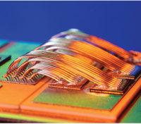
• MICRO-PATTERNING: An optically tailored resist is dispensed as a puddle on the substrate surface. By moving the substrate in contact with the stamp, the resist spreads radially between the substrate and stamp stack, filling the 3D patterning of the stamp.
• NANO-PATTERNING: A flexible stamp is bent at the centre and brought into contact with the substrate coated with resist. Contact wave extends radially to the substrate's outer edge. As a final step the resist solidifies (for example via UV illumination). The stack is then separated and the negative of the pattern features remains in the resist on the substrate.
Accurate wedge error compensation and gap setting are therefore crucial factors for imprint lithography. The SUSS mask aligner platform provides an active wedge error compensation system that employs piezo-electric linear actuators, a highly accurate gap measurement system and a force detector. This accomplishes exact lateral and axial alignment of stamp to substrate.
SCIL: Substrate Conformal Imprint Lithography is utilized for demanding imprint processes as the process provides best-in-class residual layer control for optimal etching mask definition. SCIL is available from SUSS Microtec on the MA / BA Gen4 Pro series Mask Aligner. The method combines a soft composite working stamp with a rigid glass carrier to achieve low pattern deformation. In the SCIL process, nano-imprint resist fills pattern features via capillary action; this low pressure force yields minimal pattern distortion and residual layer thickness variation. The stamp is brought into substrate contact and separated in a sequential movement, allowing fully automatic handling which avoids forces that may damage the substrate or imprinted structures. This proprietary method developed (in collaboration with Philips Research) reduces air inclusions even in large-area printing, improving structure uniformity. Excellent substrate conformity and pattern fidelity over large areas make SCIL a powerful tool for applications such as LED or VCSEL, optical gratings and MEMS (NEMS).
UV-NIL: Ultraviolet Nano-Imprint Lithography is a low-cost solution for replicating high resolution (several nanometres) structures in small areas. UV-NIL is available on SUSS Microtec's MA / BA Gen4 Pro and MJB4 series Mask Aligners. UV-NIL employs a rigid quartz stamp, which transfers structures onto a UV-sensitive resist coated substrate. The printing process is supported with SUSS Microtec's novel Wedge Error Compensation (WEC), enabling accurate levelling of the substrate to the stamp; fundamental to imprint uniformity. Stamp and substrate can also be accurately aligned while all the crucial process parameters such as pressure distance and speed can be precisely controlled, making SUSS Microtec platforms extremely versatile and ideal for R&D. Additional tooling is also suited to producing in-house low cost test stamps with sub-micron resolution.
UV-NIL technology by SUSS MicroTec delivers a valuable solution for developing of next-generation semiconductor, MEMS / NEMS and optoelectronic technology and is the ideal starter kit for Research.
See our "Knowledge Base Document" for a guide to the basics of micro and nano imprint lithography.
123PreviousNext
Imprint Lithography Technical Downloads
File
SUSS MicroTec IMPRINT Lithography Brochure
Download
Visit the Inseto (UK) Ltd website for more information on Imprint Lithography
ENQUIRY FORM