High Power Wafer Probing Equipment
Key FeaturesHigh Power Wafer Probing EquipmentTest and characterize power devices up to 10 KV or 500 AmpsManual, Semiautomatic and Fully Automatic ConfigurationsTest individual die or wafers from 100 mm to 300 mmTest using manual or programmable manipulators or probe cardsTesting in open air, immersed in fluid or in vacuumFully guarded, shielded, and interlocked safety system
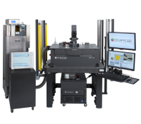
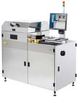
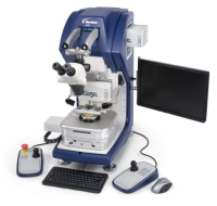
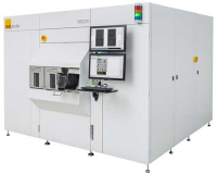
SemiProbe's High Power Wafer Probing equipment is for high voltage and high current testing of high power semiconductor wafers and devices.
The equipment is configured using the modular Probe System for Life (PS4L) platform, which allows customers to specify and purchase a system according to their exact requirements or budget limitations. Thereafter, the systems can either be upgraded or reconfigured as needs change or budgets allow.
The high power probe station is integrated with either a Dark Box or Light Curtain and will interface with Keithley, Keysight, Tesec and other test instrumentation. Dependent upon configuration, the equipment is capable of testing devices in open air, immersed in fluid or in vacuum up to 10KV and 500A (pulsed), using either high power probe arms or probe cards; lower ranges (e.g. 3KV) are also available.
Manual, semi and fully automatic versions are available for processing die through 100 to 300 mm wafers. The systems are also capable of processing thin wafers, can have enclosed wafer chucks with -65°C to 300°C range and feature an extensive range of additional options.
All high power systems are built with a fully guarded, shielded, and interlocked system to ensure user safety.
1234PreviousNext
High Power Wafer Probing Equipment Downloads
File
High Power Probe Station Overview
Download
File
SemiProbe Corporate Overview Datasheet
Download
Visit the Inseto (UK) Ltd website for more information on High Power Wafer Probing Equipment

